THIS WEBSITE USES COOKIES
We use cookies to personalise content, to provide social media features, and to analyse our traffic. By choosing 'allow all cookies', you consent to our cookies.
To find out more, read our privacy policy and cookie policy.
Report on the use of ALD towards mass production of buffer layers and contacts (D3.6, M26 - December 2024)
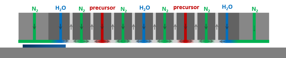
The main goal of deliverable D3.6 was to design and engineer the SnO2 deposition process by atomic layer deposition (ALD) for both temporal and spatial configurations. The researchers have also assessed the scalability of ALD towards mass production of buffer layers and contacts, by considering the state-of-the-art in batch ALD processing for crystalline silicon PV, already reported in literature for ALD of thin Al2O3 passivating layers. TUE has developed both temporal and spatial ALD SnO2 recipes at 100°C, with focus on uniformity in film thickness and refractive index. The latter is a critical metric for assessing SnO2 film quality as a buffer layer protecting the underlying layers (fullerene and perovskite) from the sputtering process of the transparent conductive oxide. TUE also evaluated the balance between film quality and ALD cycle time, which directly influence process throughput. An initial cost analysis for batch ALD processing of SnO2 has shown that the ALD Sn-precursor and therefore the SnO2 film thickness have a significant impact on the overall cost.
Schematic of a spatial ALD setup, where precursor and co-reactant are injected through separate slits into the deposition zones.
Developed by
Receive the latest news
Subscribe To Our Newsletter
Get PV industry insights and stay informed about PEPPERONI’s progress.